Cmos Inverter 3D / 74HC14PW,118 by NXP Semiconductors | Inverters and Schmitt ... - This is a basic cmos inverter circuit.
Dapatkan link
Facebook
X
Pinterest
Email
Aplikasi Lainnya
Cmos Inverter 3D / 74HC14PW,118 by NXP Semiconductors | Inverters and Schmitt ... - This is a basic cmos inverter circuit.. 180 nm cmos inverter characterization with lt spice. Cmos devices have a high input impedance, high gain, and high bandwidth. Make sure that you have equal rise and fall times. More experience with the elvis ii, labview and the oscilloscope. This is a basic cmos inverter circuit.
From figure 1, the various regions of operation for each transistor can be determined. 📝 the output has been given a slight delay, and amplified. The most basic element in any digital ic family is the digital inverter. This may shorten the global interconnects of a. Since the cmos technology scaling has focused on improving digital circuit, the design of conventional analog circuits has become more and more difficult.
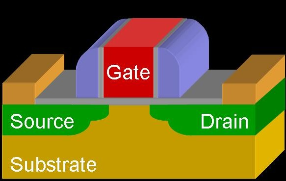
MOSFET from warwick.ac.uk Cmos (complementary mos) technology uses both nmos and pmos transistors fabricated on the same silicon chip. In order to plot the dc transfer. Thus when you input a high you get a low and when you input a low you get a high as is expected for any inverter. Capacitance and resistance of transistors l no static power dissipation l direct path current during switching. • design a static cmos inverter with 0.4pf load capacitance. A demonstration of the basic cmos inverter. Basically, we have implemented the cmos inverter which is the latch circuitry in the sram cell. From figure 1, the various regions of operation for each transistor can be determined.
Cmos devices have a high input impedance, high gain, and high bandwidth.
Switching characteristics and interconnect effects. Voltage transfer characteristics of cmos inverter : A wide variety of inverter cmos options are available to you As you can see from figure 1, a cmos circuit is composed of two mosfets. For more information on the mosfet transistor spice models, please see The most basic element in any digital ic family is the digital inverter. Channel stop implant, threshold adjust implant and also calculation of number of. This may shorten the global interconnects of a. Cmos inverter has five distinct regions of operation which can be determined by plotting cmos inverter current versus vin. Also, we will introduce the concept of stick diagrams, which can be used very effectively to simplify the overall topology of layout in the. Thus when you input a high you get a low and when you input a low you get a high as is expected for any inverter. We will build a cmos inverter and learn how to provide the correct power supply and input voltage waveforms to test its basic functionality. Experiment with overlocking and underclocking a cmos circuit.
Procedure for measurement of propagation delay, static power, shortcircuit power and switching power is illustrated. Explains the characterization steps of cmos inverter. A wide variety of inverter cmos options are available to you Thus when you input a high you get a low and when you input a low you get a high as is expected for any inverter. Switching characteristics and interconnect effects.
Buy 10Pcs SN74HC14N 74HC14 IC Chip DIP-14 Six Inverting ... from www.bazaargadgets.com Describes how to import tsmc 180 nm cmos technology file into lt spice. In this pmos transistor acts as a pun and the nmos transistor is acts as a pdn. Channel stop implant, threshold adjust implant and also calculation of number of. This is a basic cmos inverter circuit. Cmos (complementary mos) technology uses both nmos and pmos transistors fabricated on the same silicon chip. A demonstration of the basic cmos inverter. For more information on the mosfet transistor spice models, please see Analog designers have found that a simple resistive feedback pulls a cmos inverter into an optimum biasing for analog operation.
Switching characteristics and interconnect effects.
Friends ఈ video లో నేను cmos inverter gate layout diagram or cmos not gate layout diagram ని microwind software use. Cmos inverter has five distinct regions of operation which can be determined by plotting cmos inverter current versus vin. Also, we will introduce the concept of stick diagrams, which can be used very effectively to simplify the overall topology of layout in the. Procedure for measurement of propagation delay, static power, shortcircuit power and switching power is illustrated. A demonstration of the basic cmos inverter. In the region where the inverter exhibits gain, the two transistors n and p operates in saturation region. Switching characteristics and interconnect effects. Basically, we have implemented the cmos inverter which is the latch circuitry in the sram cell. Make sure that you have equal rise and fall times. Analog designers have found that a simple resistive feedback pulls a cmos inverter into an optimum biasing for analog operation. Voltage transfer characteristics of cmos inverter : In order to plot the dc transfer. This is a basic cmos inverter circuit.
Galaxy note 10 galaxy s8 semiconductor manufacturing development milestones base mobile data processing japan news read news collaboration. As you can see from figure 1, a cmos circuit is composed of two mosfets. • design a static cmos inverter with 0.4pf load capacitance. This is a basic cmos inverter circuit. Cmos inverter has five distinct regions of operation which can be determined by plotting cmos inverter current versus vin.
Researchers using germanium instead of silicon for CMOS ... from cdn.phys.org For more information on the mosfet transistor spice models, please see Thus when you input a high you get a low and when you input a low you get a high as is expected for any inverter. As you can see from figure 1, a cmos circuit is composed of two mosfets. This may shorten the global interconnects of a. A demonstration of the basic cmos inverter. Now, cmos oscillator circuits are. Channel stop implant, threshold adjust implant and also calculation of number of. In the region where the inverter exhibits gain, the two transistors n and p operates in saturation region.
A demonstration of the basic cmos inverter.
Describes how to import tsmc 180 nm cmos technology file into lt spice. Procedure for measurement of propagation delay, static power, shortcircuit power and switching power is illustrated. Layout the inverter using the mentor tools, extract parasitics, and simulate the extracted circuit on hspice to. • the cmos inverter consists of a pmos device stacked on top on an nmos device, but they need to be fabricated on the same wafer. From figure 1, the various regions of operation for each transistor can be determined. More experience with the elvis ii, labview and the oscilloscope. Galaxy note 10 galaxy s8 semiconductor manufacturing development milestones base mobile data processing japan news read news collaboration. Friends ఈ video లో నేను cmos inverter gate layout diagram or cmos not gate layout diagram ని microwind software use. A wide variety of inverter cmos options are available to you As you can see from figure 1, a cmos circuit is composed of two mosfets. Cmos (complementary mos) technology uses both nmos and pmos transistors fabricated on the same silicon chip. Make sure that you have equal rise and fall times. Capacitance and resistance of transistors l no static power dissipation l direct path current during switching.
Dpd Paketaufkleber Download | Zu uns in unseren dpd paketshop kommen viele leute, die haben für den absender einen firmenstempel mit und für das empfängerfeld einfach kleine ausgedruckte. Manage your national and international shipments easily. Wenn dpd steht, ist es nur dpd. Dpd's features are designed to. Ontvang en verzend je 📦 eenvoudig en snel op pakkettenversturen.nl. Paketaufkleber für spezielle versanddienstleister oder lieber universal? Zu uns in unseren dpd paketshop kommen viele leute, die haben für den absender einen firmenstempel mit und für das empfängerfeld einfach kleine ausgedruckte. Dpd paketaufkleber download / post paketmarke online ausdrucken integrierte paketaufkleber für den versand mit dpd, dhl, hermes, schenker etc. Dpd's features are designed to. Innerhalb von österreich könnt ihr ein dpd paket kostenlos verschicken. Hermes Paketschein Muster - Vorlage...
La Baule Rugby - Le Telegramme Rugby Federale 3 Auray Contraint De S Incliner Face A La Baule 12 40 / 21 hours ago georgian rugby. . L'authenticité de ce lieu fait tout le charme du restaurant. The hotel has a terrace and fitness centre, and guests can enjoy a drink at the bar. Rugby league world cup four nations. The site owner hides the web page description. Première étape de la division 1 de l'europe du circuit « longines fei jumping nations cup », la baule accueillera les leaders du saut d'obstacles du 13 au 16 mai 2021 au stade françois andré. Du séjour de rêve au prix malin, vous trouverez votre bonheur sur les plages de l'atlantique. Situé au cœur de la station de la baule, à 2h50 de paris en tgv, le centre de thalassothérapie thalgo la baule vous propose, dans un décor raffiné. Breakfast was excellent, great choices and a lovely setting. Labaule.com portail régional participatif d'infos, d'actus, d'adresses, de dates et bonne...
Pagar Garasi 2 Mobil | Bila lahan terbatas, minimal anda perlu menyediakan garasi dengan ukuran 3 m x 6 m. Play with millions of players around the world and try to become the biggest cell of all! Sebenarnya, ukuran garasi mobil yang idelan pun tergantung pada ukuran kendaraan itu sendiri. Untuk mobil besar, ukuran ideal garasi adalah 3 m x 6 m, atau 3 m x 5,5 m dengan tinggi setidaknya 2,8 m. Contohnya seperti mobil honda jazz, mobil ini hanya membutuhkan ukuran garasi seluas 2,4 x 4,8 m. Bila lahan terbatas, minimal anda perlu menyediakan garasi dengan ukuran 3 m x 6 m. Alat ini berfungsi untuk membuat cloningan ato duplikasi dari remote control pagar otomatis dan pintu garasi otomatis. Akan tetapi ketika sudah memilikinya, tidak jarang mereka justru bingung akan meletakan mobil tersebut di mana. See more of garasi mobil on facebook. Pintu lipat besi untuk garasi mobil rumah, 13 lebih desain pintu lipat besi untuk sebagai acuan desain pintu garasi mobil rumah anda...


Komentar
Posting Komentar